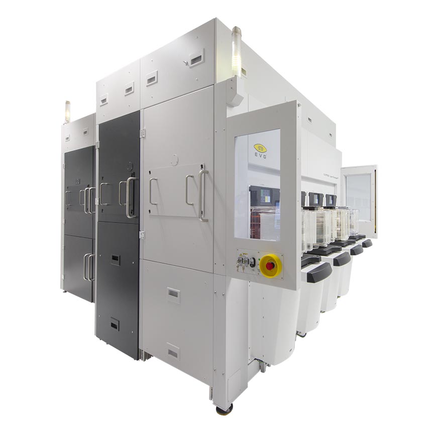
The EVG®880 LayerRelease™ System is a fully automated system and enables precise release of layers from silicon carrier substrates using an IR laser.
The EVG®880 LayerRelease™ System enables nanometer–precision release of bonded, deposited or grown layers from silicon carrier substrates using an infrared (IR) laser coupled with specially formulated inorganic release materials in a proven, high–volume–manufacturing (HVM) capable platform.
The innovative process eliminates the need for glass substrates and organic adhesives overcoming the temperature limitations resulting in front–end process compatibility for ultra–thin layer transfer and downstream processes.
Enabling silicon carriers with inorganic release layers avoids these temperature and glass carrier compatibility issues. In addition, the nanometer precision of IR laser-initiated separation allows for processing extremely thin device wafers without changing processes of record. Subsequent stacking of such thin device layers enables higher–bandwidth interconnects and new opportunities to design and segment dies for next–generation, high–performance devices.
The EVG 880 LayerRelease System is based on the same platform as EVG’s industry–leading EVG®850 series of automated temporary bonding/debonding and silicon–on–insulator (SOI) bonding systems, with a compact design and HVM proven wafer handling system.
Features
-
Product Features
- Fully automated, front end compatible HVM equipment.
- Substrate size up to 300 mm (SEMI M1).
- Substrate ID reader and SECS/GEM integration.
- ISO 3 environment.
- Complete process control including laser metrology at point of use.
- Integrated Separation Module for separation of exposed substrates.
-
3D Integration | Scaling Roadmap:
- Scalpel-like precision of IR laser triggered film release through silicon wafers
- Enables novel, revolutionary 3D integration process flows for ultra-thin layer stacking by fusion and hybrid bonding
- Integrates with any hybrid and fusion bonding process combination for advanced device manufacturing and 3D stacking
- Use of existing FEOL materials, processes and infrastructure
- Transfer layer uniformity is defined by epitaxy uniformity eliminating uniformity limitations from standard wafer thinning processes such as wafer grind, polish and etching
- Universal material transfer in combination with fusion bonding of III-Vs, 2D materials, superlattices, etc.
-
Heterogeneous Integration:
- Enabling silicon carrier wafers as temporary carriers
- Enables use of standard and established process technology, eliminating the need for adapted low temperature processes due to carrier triggered temperature limitations
- Enables Processing of ultrafine pitch redistribution layer patterning on silicon substrates with leading lithography methods
- No need for costly equipment updates or backside deposition to enable glass wafer processing and chucking
Talk to our EVG product experts!
Questions?
Related technologies
Questions about our products and technologies?
Contact the EVG experts